Exploring the 2026 MicroLED revolution that marks the end of the OLED era. We dive into the microscopic architecture of inorganic Gallium Nitride (GaN) crystals that solve the "AR Brightness Crisis" with outputs exceeding 4 million nits. The article covers breakthroughs at MWC 2026, the "Griffin" automotive holography platform, and manufacturing triumphs in Mass Transfer yields. Finally, we examine how MicroLED serves as the catalyst for the transition from smartphones to unbounded spatial computing.
Part 1: Introduction and The Great Brightness Crisis in Augmented Reality
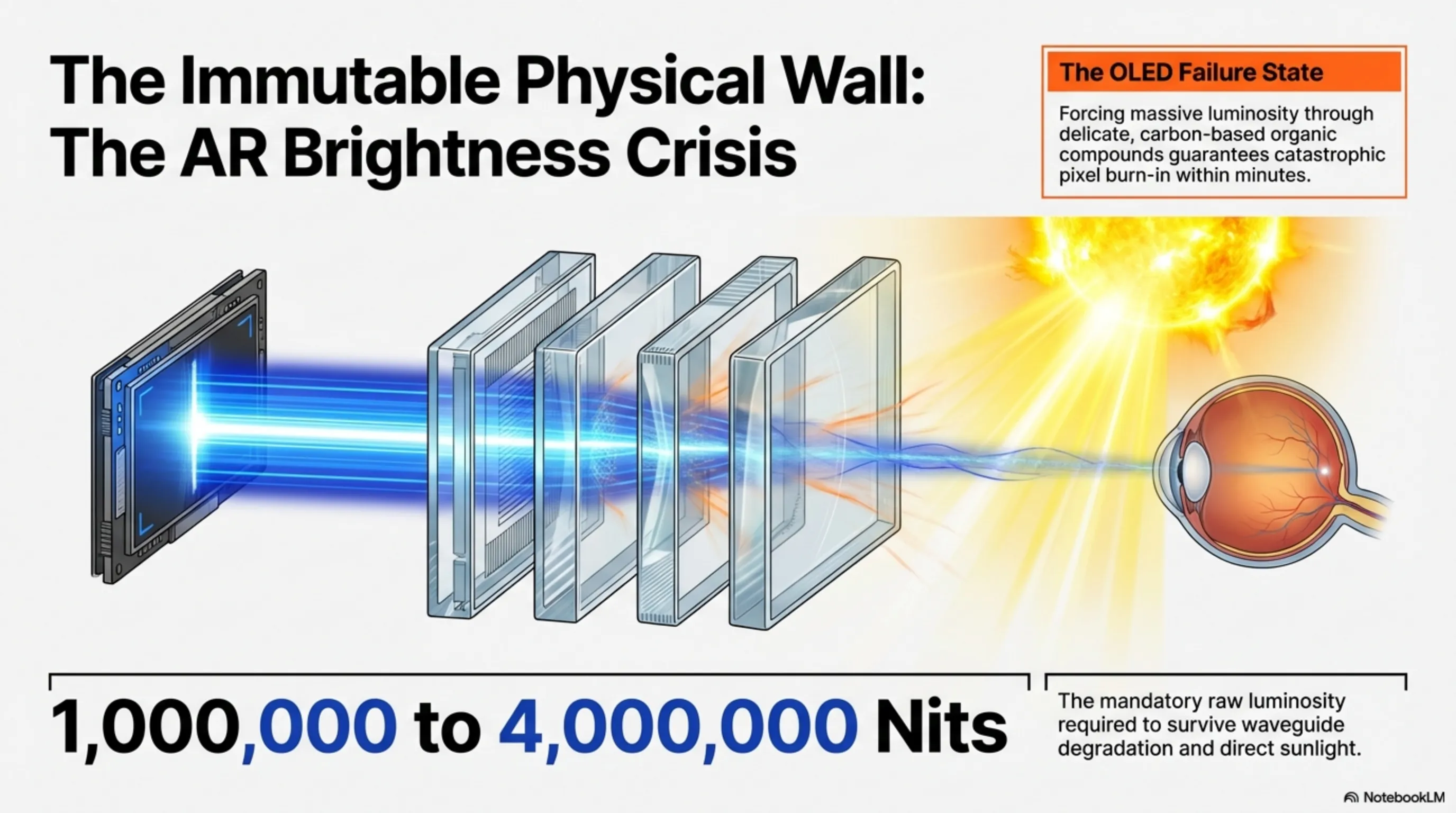
For several highly intense and incredibly expensive years, the absolute holy grail for Silicon Valley hardware engineers and consumer electronics designers has unequivocally been the development of authentic Augmented Reality (AR) smart glasses. The ultimate, unwavering objective was to completely engineer a device physically analogous to standard prescription spectacles or conventional Ray-Ban sunglasses, yet fiercely capable of actively projecting three-dimensional user interfaces, critical smart notifications, and entirely volumetric, live holograms directly into the user's immediate physical field of view. Unfortunately, up until late 2025, every colossal attempt executed by technology behemoths such as Apple (with their intensely heavy Vision Pro headset, an architecture we radically dissected in earlier deep dives) and Meta violently collided with a brutally uncompromising, concrete wall constructed directly out of the immutable physical laws governing light: The Brightness Crisis under direct sunlight.
Micro-OLED displays organically represented the absolute pinnacle of available visual technology prior to the explosive breakthroughs of 2026. While they flawlessly delivered unparalleled, staggering contrast ratios and achieved absolute, infinite black levels by entirely shutting down localized pixels, they possessed one deeply fatal, inherently physical weakness: The organic carbon-based compounds constituting OLED structures inevitably and rapidly suffer from the devastating phenomenon of pixel "Burn-in" when aggressively forced to sustain excessively high electrical currents to generate massive luminosity.
Because authentic AR glasses are fundamentally designed for continuous, all-day utilization in harsh outdoor environments directly beneath the blinding glare of the afternoon sun, their internal micro-displays must harbor the terrifying capability to "throw" holographic images with a mind-numbing raw luminosity resting somewhere between 1,000,000 and 4,000,000 Nits (Candelas per square meter). This violent burst of light is absolutely mandatory because the image must forcibly travel through and inevitably degrade within complex, densely stacked optical Waveguide lenses before the residual photons finally reach the human retina in a perceivable, intelligible state. OLEDs, bound inherently by their fragile organic chemistry, never possessed the physical durability to achieve these agonizing brightness levels without literally melting the panel or entirely incinerating their own organic sub-pixels within minutes. In March 2026, the global hardware ecosystem, spearheaded by the final industrial maturation of MicroLED panels, officially and aggressively announced the absolute termination of this historical physical limitation.
Part 2: The Microscopic Autopsy: MicroLED vs. OLED vs. LCD Architectures
To deeply and authentically comprehend the sheer engineering majesty inherent within MicroLED technology, we must rigorously analyze its foundational structure at the extreme nanometer scale. Classical Liquid Crystal Displays (LCDs) structurally demanded a thick, unified background backlight array, aggressively overlaid with complex, highly restrictive plastic liquid crystals and dense polarizing color filters. This archaic, deeply layered architecture rendered them inherently bulky, painfully power-hungry, and entirely incapable of rendering authentic, true-black contrast since the backlight perpetually bled through the liquid shutters.
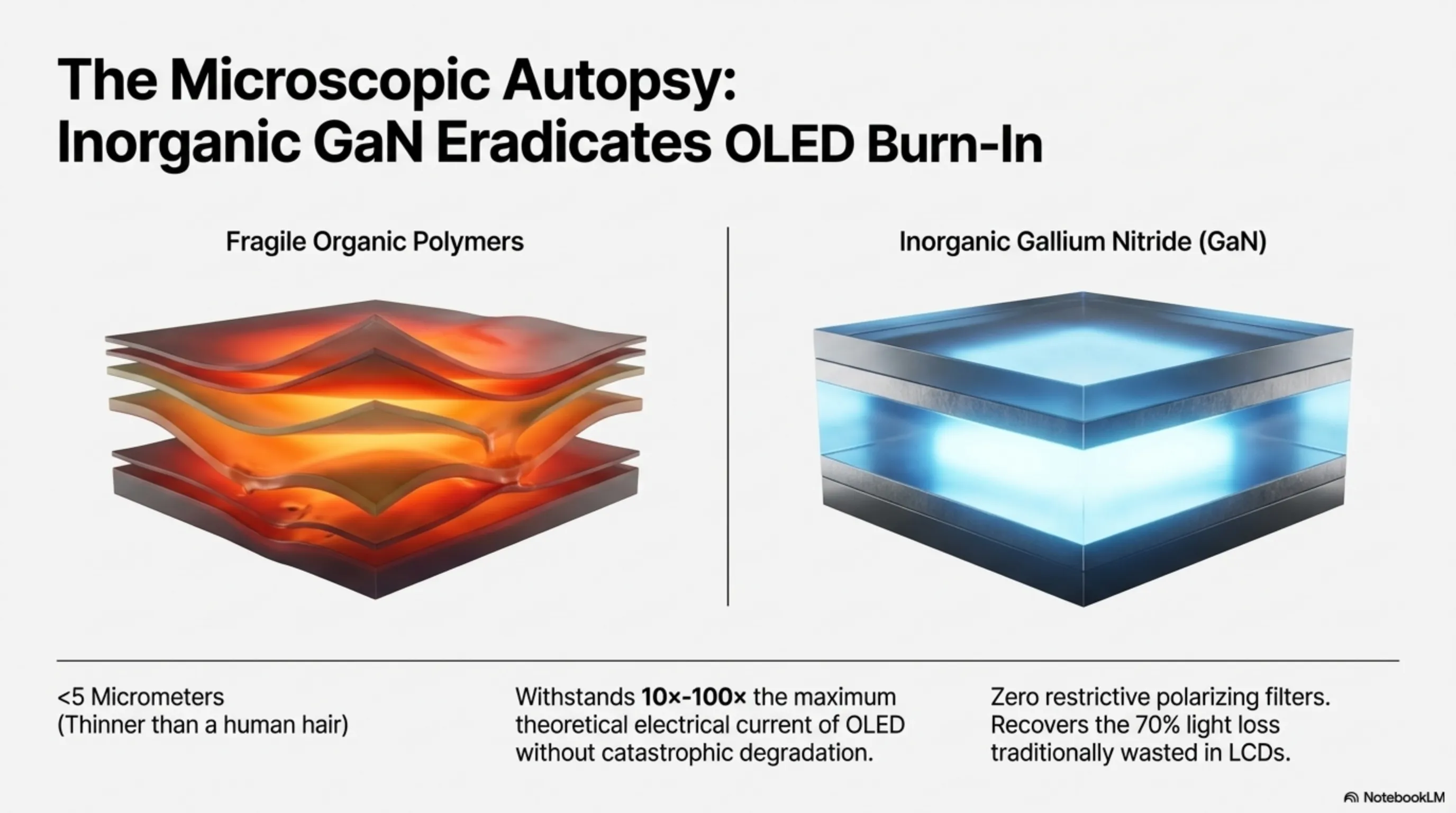
The revolutionary OLED (Organic Light Emitting Diode) technology forcefully disrupted the market by entirely amputating the need for a unified backlight. It introduced organic, self-emissive pixels that generated their own localized light and color—a breathtaking leap forward. However, the bitter reality remained that these delicate organic polymers biochemically degrade and permanently decay over continuous temporal exposure, especially when driven fiercely by high voltages.
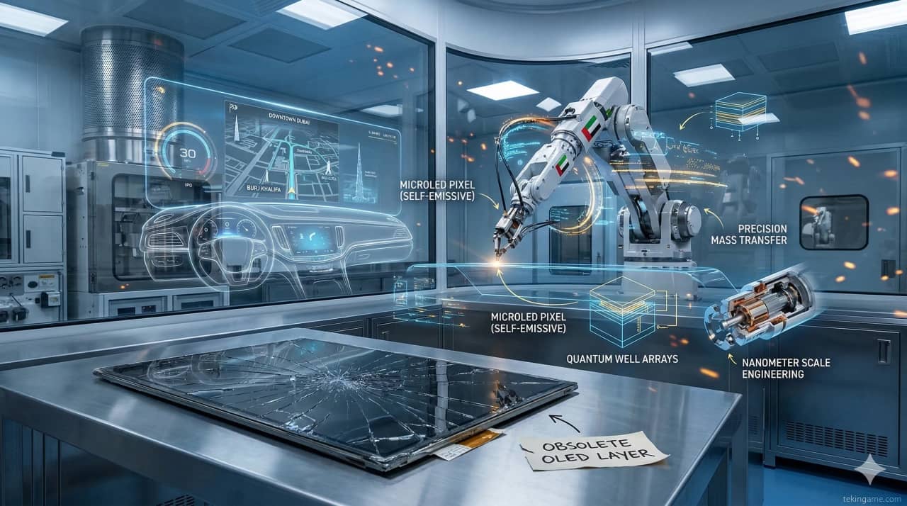
MicroLED (Microscopic Light Emitting Diodes) technology brilliantly inherits the absolute best foundational characteristic of OLED: it consists entirely of flawlessly self-emissive, independently stoppable pixels. However, the shocking, paradigm-shifting distinction lies directly in its material chemistry. Instead of utilizing vulnerable, squishy organic polymers, the MicroLED architecture is ruthlessly constructed using incredibly robust, massively resilient inorganic (mineral) crystalline structures, predominantly Gallium Nitride (GaN). The physical footprint of every single one of these individual optical diodes often completely fails to exceed an agonizingly small 5 micrometers—making them substantially thinner than a single strand of human hair.
These exceptionally hardened inorganic materials physically possess an entirely terrifying capacity for electrical and thermal tolerance. A singular MicroLED sub-pixel can effortlessly, continuously withstand a flowing electrical current equivalent to tens or even hundreds of times the maximum theoretical tolerance of a comparable OLED pixel, executing this without the slightest infinitesimal risk of triggering a catastrophic, irreversible Burn-in event. The direct, violent result of this extreme durability is the generation of utterly incomprehensible levels of optical brightness. These displays effortlessly maintain rendering holographic interface elements that remain radically crisp, flawlessly brilliant, and vividly lucid even while the user is staring directly into the punishing reflection of a sun-drenched Middle Eastern desert.
Furthermore, compounding this colossal advantage, because the architectural design absolutely dictates the complete eradication of heavily restrictive polarizing color filters—which traditionally blocked and wasted up to 70% of generated light in LCDs—the raw optical efficiency coefficient of this structure is astronomically high. This translates to an unprecedented, almost unbelievable reduction in total battery drain, finally solving the ultimate power-draw equation for ultra-lightweight, all-day wearable smart glasses.
Part 3: The Technological Shockwave of MWC 2026: TCL CSOT's 0.05-inch Display
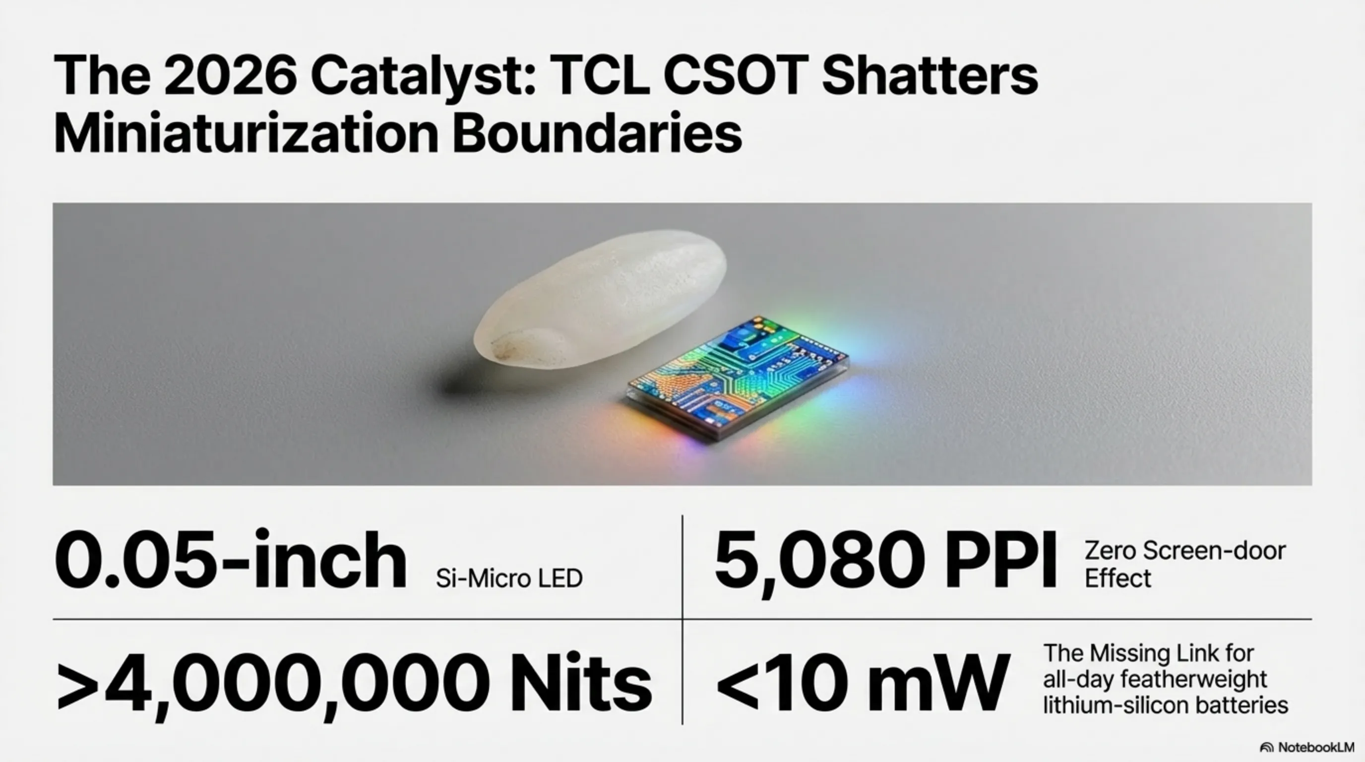
The Mobile World Congress (MWC) hosted in Barcelona during March 2026 served as the violently contested battleground where global semiconductor and panel manufacturing titans flexed their absolute manufacturing supremacy. However, the singular hardware event that unceremoniously stole the oxygen from the entire convention floor belonged undeniably to the TCL CSOT (China Star Optoelectronics Technology) pavilion. This corporation brutally shattered the universally accepted physical boundaries of extreme hardware miniaturization. They brazenly unveiled the "World's Smallest Silicon-based Micro LED (Si-Micro LED) Display"—an active, fully functional rendering panel possessing physical dimensions measuring a mere 0.05 inches diagonally (visually smaller than half a grain of standard rice)!
The raw, heavily audited statistical metrics surrounding this microscopic piece of silicon read exactly like an excerpt from advanced science fiction. This practically invisible display boasts a truly terrifying, hyper-dense pixel concentration of 5,080 Pixels Per Inch (PPI). To contextualize this aggressive density, it dictates that even when heavily magnified through thick AR waveguide lenses, the naked human eye will observe impeccably smooth, entirely cohesive curves on the sharpest typography, experiencing absolutely zero discernible "Screen-door Effect" (the ugly observation of gaps between pixels).
Yet, the genuinely shock-inducing facet of this historical unveiling was its raw photon output. Despite its absurdly compressed nano-metric footprint, this specific panel is physically capable of actively blasting a blinding, retina-searing luminosity exceeding 4,000,000 Nits (Four Million Nits). Even more staggering is the power telemetry: while generating this colossal light wave, its total energy consumption while operating at standard projection baselines remains firmly crushed below 10 milliwatts (mW).
These deeply advanced Si-Micro LED optical sensors represent the exact, highly coveted engineering "Missing Link" required for the immediate commercial deployment of genuine "All-day Battery Life" smart glasses. Hardware manufacturers can finally conceal incredibly tiny, featherweight lithium-silicon battery cells seamlessly within the thin sunglass stems, yet still confidently command the headset to vividly render interactive navigation arrows, live email tickers, and entirely volumetric holographic video calls brightly under the unforgiving noon sun.
Part 4: Solving the Optic Frequency Blindness: Epitaxial Engineering and InGaN Quantum Wells
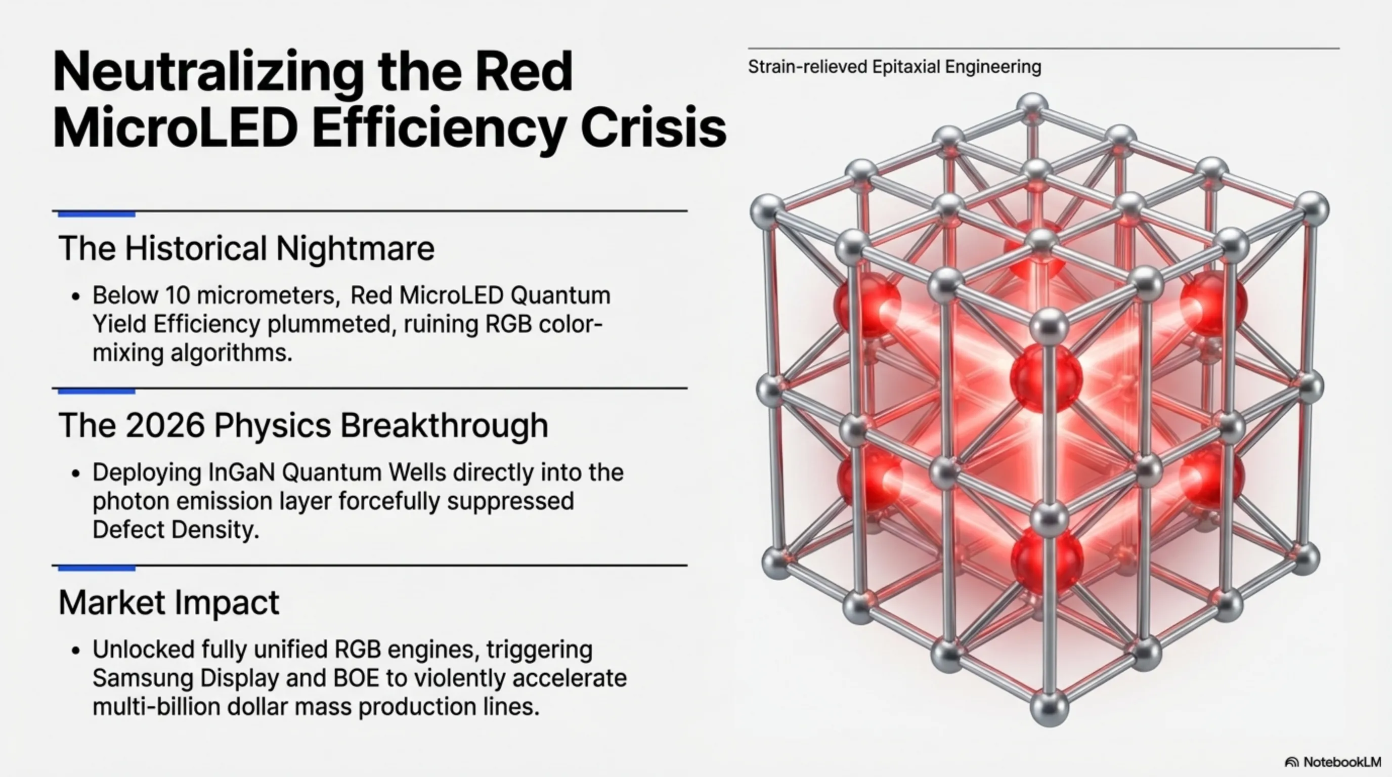
Throughout the deeply grueling, painfully expensive multi-year Research and Development (R&D) process, fabricating the fundamental blue and green micro-pixels utilizing standard Gallium Nitride (GaN) materials scaling down to micro-dimensions was comparatively straightforward for material physicists. However, the successful fabrication of the "Red" pixel operating at scales brutally shrinking below 10 micrometers rapidly evolved into a deeply notorious, industry-wide nightmare formally dubbed the "Red MicroLED Efficiency Crisis." For nearly half a decade, this specific spectral issue plagued optical engineers. As the physical structure of the red emitting diode contracted into microscopic dimensions, its underlying Quantum Yield Efficiency plummeted catastrophically. The diodes inherently became incredibly weak, severely dim, and massively unresponsive. This violently destructive imbalance routinely caused the precise color-mixing algorithms—required to generate pure, unified white light within the final AR image—to fail miserably, rendering the displays unusable for professional visual applications.
In the twilight weeks of 2025 and accelerating rapidly into early 2026, elite material scientists engaged deeply in this sector achieved an earth-shattering physical breakthrough. By aggressively deploying highly advanced "Strain-relieved Epitaxial Engineering" techniques—fundamentally manipulating the atomic lattice structure of the semiconductor material during its intensely hot formation phase—they successfully integrated entirely novel structural anomalies known as "Indium-Gallium-Nitride (InGaN) Multiple Quantum Wells" directly into the photon emission layer.
This aggressively innovative, heavily microscopic approach overwhelmingly neutralized and forcefully suppressed the devastating "Defect Density" anomalies previously rampant within the crystal structures of the red diodes. The monumental result was that ultra-miniature, nano-scale red MicroLEDs finally, dependably succeeded in generating the absolute quality, the deep spectral color purity, and, most crucially, the sheer explosive brightness output perfectly synchronized and equivalently leveled with their green and blue counterparts. This monumental scientific triumph, birthed inside deeply sterile cleanroom laboratories, served as the ultimate golden key. It definitively and commercially unlocked the physical possibility of manufacturing completely unified, intensely compact Full-Color (RGB) MicroLED display engines. This precise breakthrough instantly triggered massive conglomerate display manufacturers, highly notably Samsung Display and BOE Technology, to violently accelerate their schedules and rapidly ignite their multi-billion dollar Mass Production lines.
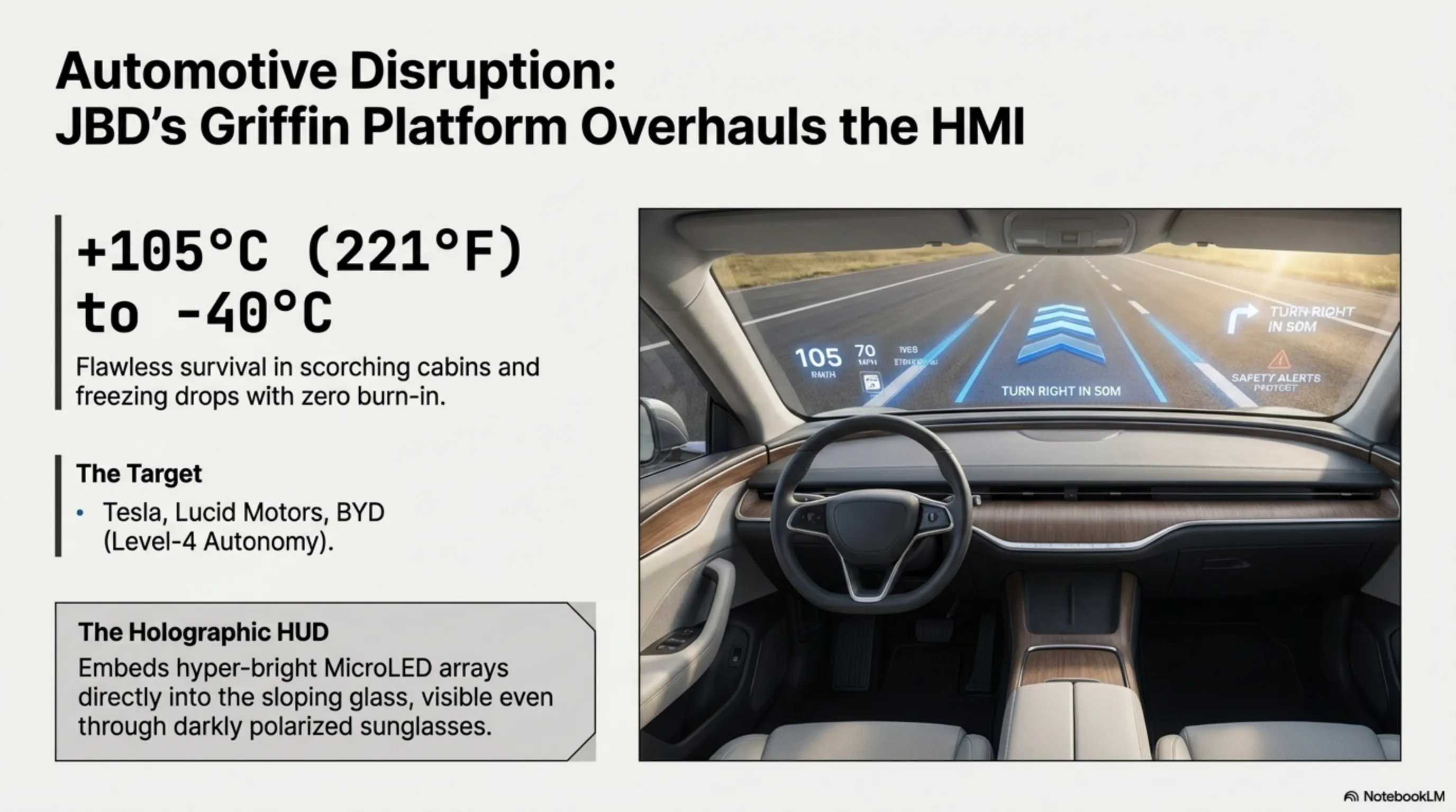
Part 5: The EV Industry and JBD's Griffin Platform: Windshield Holography
The spectacular implications of the MicroLED revolution are fundamentally not restricted merely to augmenting the wearable technology and headset ecosystem; its transformative potential acts as a massive disruption vector aimed directly at completely overhauling the Human-Machine Interface (HMI) within the global automotive industry. The highly pioneering Chinese corporation JBD (Jade Bird Display)—a monolithic entity historically specializing exclusively in fabricating micro-panels for Near-Eye glasses—aggressively shocked the automotive sector in the Spring of 2026 by forcefully unveiling their deeply integrated proprietary automotive platform code-named "Griffin." This sophisticated hardware matrix directly, unapologetically targets elite manufacturers producing luxury Electric Vehicles (EVs) and Level-4 Autonomous driving platforms, notably courting giants such as Tesla, Lucid Motors, and BYD.
The core engineering philosophy driving the Griffin platform is the deep, structural embedding of microscopic, hyper-bright MicroLED arrays directly into the internal projection matrices of next-generation Head-Up Displays (HUD) and actively integrating them deep within the sloping glass of the automotive windshield itself. Because MicroLED elements flawlessly harbor undisputed, uncontested brightness superiority combined with piercing color purity, critically vital driving telemetry—such as live dynamic dashboard metrics, active route navigation arrows physically "painted" onto the actual tarmac of the road ahead, severe emergency braking warnings, and richly detailed holographic welcome interfaces—can now be forcefully projected onto the windshield glass. Astonishingly, these volumetric projections remain utterly and aggressively visible to the driver even under the most punishing, blindingly intense external lighting conditions, and crucially, remain perfectly legible even while the end-user is wearing heavy, darkly polarized sunglasses.
The initial Griffin I display panels, whose rigorously classified alpha prototypes were discreetly shipped to elite automotive software developers in mid-2026, aggressively demonstrated their ability to withstand the absolute highest, most brutal degrees of Automotive-Grade Reliability. These silicon components actively endured excruciating thermal stability stress tests, functioning flawlessly inside scorching vehicle cabins at a blistering 105 degrees Celsius (221 Fahrenheit) and surviving freezing drops to minus 40 degrees Celsius, all without exhibiting even a microscopic hint of pixel degradation or burn-in. This aggressive platform is currently, actively transitioning the archaic design concept of heavy, physical digital dashboard screens toward an era totally dominated by completely invisible, highly contextual holographic images seamlessly overlaid upon the vehicle's sweeping glass surfaces.
Part 6: The Manufacturing Nightmare: Mass Transfer Yields and Laser Assembly in H2 2026
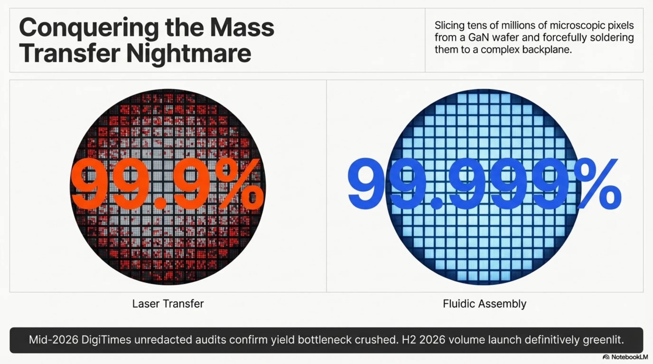
Despite an overwhelming cascade of breathtaking successes achieved within hyper-controlled, deeply sanitized laboratory environments, the absolute final, towering obstacle impeding the total takeover of the MicroLED ecosystem in 2026 revolved around its terrifyingly complex commercialization: The violently difficult industrial process known as "Mass Transfer." To comprehend this nightmare, imagine the robotic assembly of a single, premium 8K display panel. Tens of millions of fully independent, entirely microscopic pixels (which have been physically ripped and sliced off a highly expensive, monolithic Gallium Nitride growth wafer) must flawlessly, intricately find their precise picometer-level corresponding attachment bumps. They must then be swiftly carried by robotic appendages and forcefully soldered onto a massive, complex electronic Backplane circuit board.
If, during the intensely rapid and highly violent mechanical placement of 20 million microscopic pixels, the assembly robots manage to achieve an absurdly high, practically miraculous mechanical success rate of 99.9 percent, the brutal mathematical reality dictates that roughly 20,000 completely dead, permanently burnt-out pixels will brutally pepper the final consumer display—a catastrophic, un-sellable disaster representing thousands of dollars in wasted wafer silicon. In the agonizingly tense months leading up to 2026, leading Taiwanese and South Korean foundries heavily deployed immensely advanced robotics, incredibly esoteric "Laser Transfer" techniques (using rapid pulses of laser light to violently blast pixels from the wafer directly into their exact sockets), and highly controversial "Fluidic Assembly" solutions (floating pixels in precise liquid suspensions over the backplane). Through these Herculean efforts, they miraculously managed to violently crush this fatal error rate, driving the "Yield Rate" up to a commercially viable 99.999 percent.
Deep supply chain audits and unredacted logistical reports aggressively surfacing from the Taiwanese electronics media powerhouse DigiTimes in mid-2026 explicitly confirmed the momentous victory. Global display brands have finally, definitively choked out the massive production bottleneck known fundamentally as the "Yield Issue." The highly anticipated Mass Production (MP) schedules for the absolute first generation of purely consumer-focused, ultra-lightweight, socially acceptable Augmented Reality smart glasses—hardware completely armed with these flawless Asian MicroLED display engines—has been definitively, irreversibly greenlit. They are aggressively targeted for a massive, multi-million unit global volume launch scheduled solidly for the second half of the year (H2 2026).
Part 7: Supply Chain Dynamics: The Taiwanese Monopoly on Mass Production
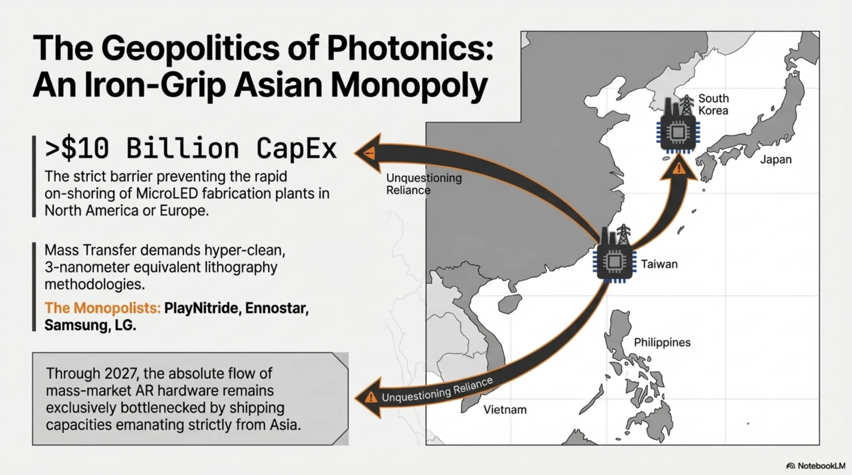
Understanding the complete macro-economic landscape of the 2026 MicroLED explosion requires a deeply cynical, highly accurate assessment of global manufacturing geography. The brutal reality of modern hardware production dictates that creating these microscopic photonic engines is not a democratic process; it is heavily monopolized. Enormous foundries based almost exclusively in Taiwan and South Korea—specifically entities like PlayNitride, Ennostar, and the display divisions of Samsung and LG—currently hold an iron grip over the massively expensive, highly classified Mass Transfer lithography machines required to fuse Gallium Nitride wafers onto silicon backplanes without destroying them.
This aggressively concentrated supply chain triggers immense geopolitical friction. Because producing MicroLED arrays demands practically the identical, hyper-clean semiconductor fabrication methodologies used to etch 3-nanometer compute processors at TSMC, Western technology giants (ranging from Apple pushing their Vision development roadmap, to Google drafting their Iris project revivals) are once again forced into unquestioning, total reliance on Asian manufacturing supremacy. The sheer Capital Expenditure (CapEx) required to build a single, functional MicroLED fabrication plant from scratch in North America or Europe easily breaches the $10 Billion threshold, making rapid on-shoring of this specific optical tech practically impossible for at least the next half-decade. Consequently, through 2026 and 2027, the absolute flow of mass-market AR hardware remains exclusively bottlenecked by the shipping capacities and yield stability emanating strictly out of the South China Sea.
Part 8: Global Mixed Reality (MR) Market Integration and Enterprise Scaling
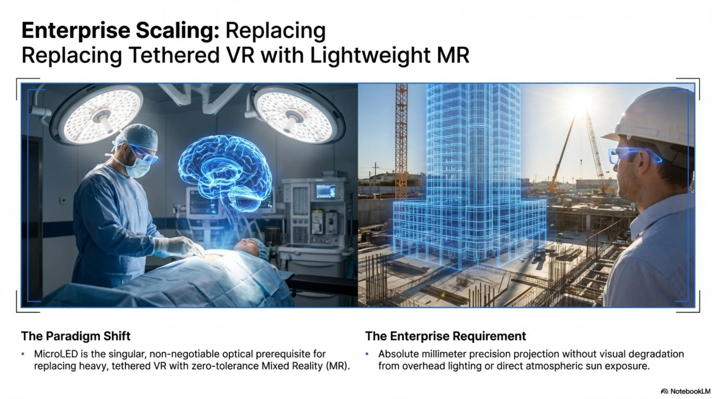
The immediate, aggressive integration of MicroLED technology rapidly transcends the consumer 'gadget' space, viciously bleeding into high-stakes, multi-billion dollar Enterprise scaling operations. Global architectural firms, advanced surgical medical centers, and complex aerospace defense contractors are actively abandoning heavy, tethered VR environments for the absolute lightweight mobility of MicroLED-powered Mixed Reality (MR).
For an elite surgeon operating in Dubai or a structural engineer assessing a high-rise foundation in Tokyo, the ability to wear practically weightless glasses that instantaneously overlay dense, intensely bright 3D MRI scans or highly detailed architectural blueprints with absolute millimeter precision over the physical patient or worksite—without losing visual clarity due to overhead surgical lights or direct sun exposure—is not merely a convenience; it fundamentally re-writes the Standard Operating Procedure (SOP) of global industries. The MicroLED architecture is the singular, non-negotiable optical prerequisite allowing MR hardware to successfully penetrate the uncompromising, zero-tolerance environments of the heavy enterprise sector.
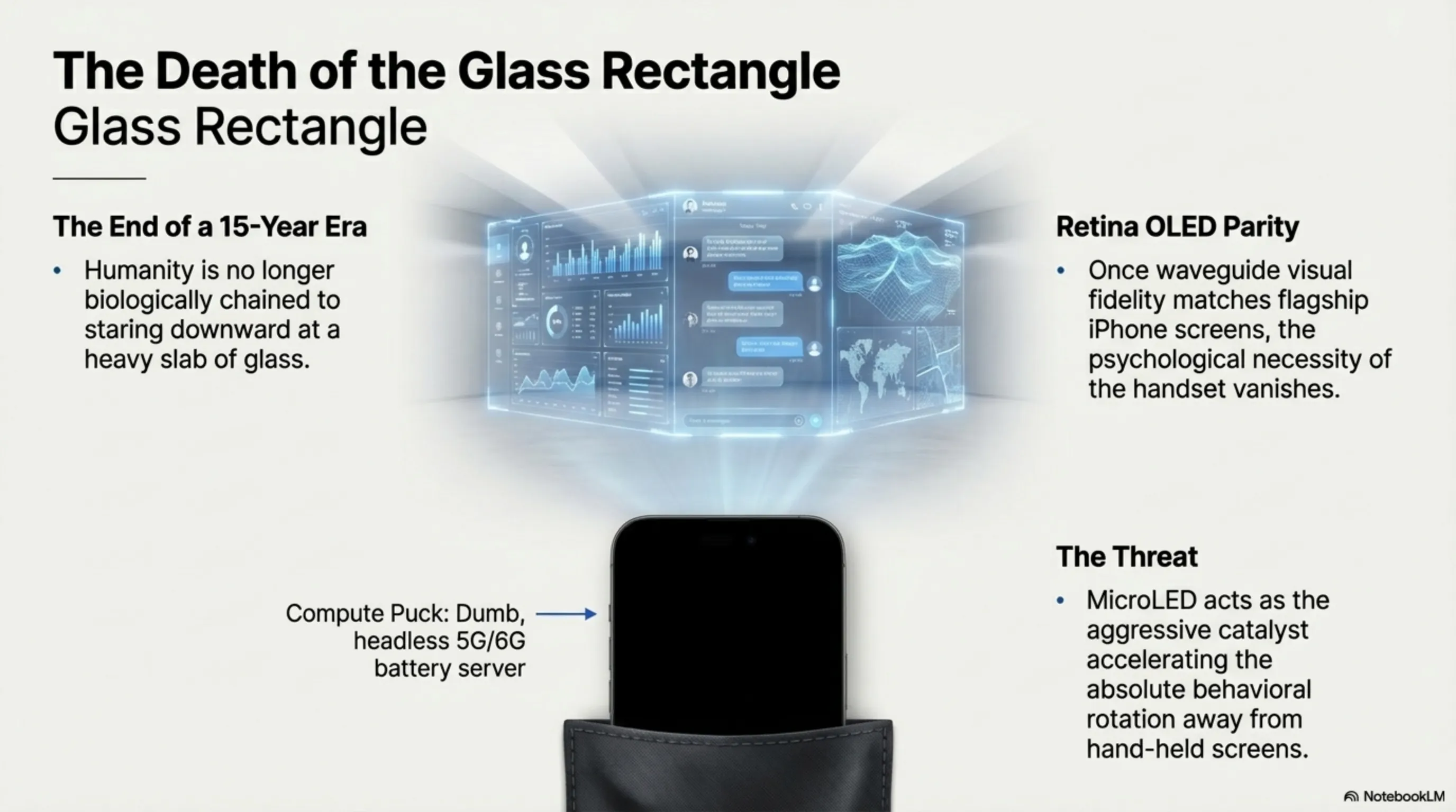
Part 9: The End of the Smartphone Era? Replacing the Glass Rectangle
The successful miniaturization of extreme-brightness panels inevitably forces a massive, deeply existential question upon the global hardware ecosystem: Does a fully matured MicroLED AR glasses market signify the absolute, violent termination of the traditional smartphone? For fifteen years, humanity has been biologically chained to staring downward into a heavy, glowing rectangular slab of glass. However, the 2026 hardware paradigm brutally suggests that smartphones are rapidly evolving merely into pocketized "Compute Pucks"—dumb, headless servers providing battery and 5G/6G cellular uplinks, while the actual, primary visual interface entirely migrates to the sweeping volumetric space surrounding the user's face.
Once the visual fidelity of a MicroLED projection reflecting inside a lightweight waveguide lens perfectly matches the visual acuity of a flagship iPhone's Retina OLED screen, the psychological and physical necessity of retrieving a bulky handset from a pocket simply vanishes. Incoming video calls, sprawling messaging threads, complex mapping applications, and infinite social media feeds simply float in the ambient physical space, rendered with crystalline, daylight-piercing perfection. The 2026 MicroLED breakthrough acts as the highly aggressive catalyst accelerating this massive behavioral rotation away from hand-held screens, directly threatening to completely cannibalize the highly lucrative, deeply entrenched trillion-dollar global smartphone market within the next five years.
Part 10: Return on Investment (ROI): Why Tech Giants Are Burning Billions on Photon Research
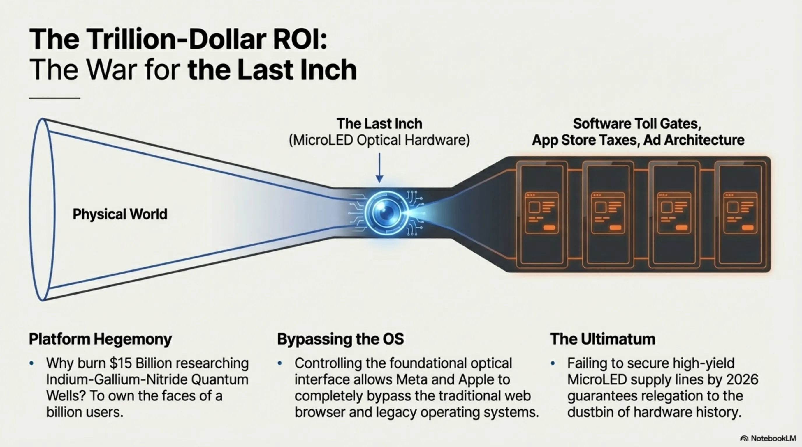
Why are tech conglomerates systematically burning through hundreds of billions of dollars dissecting crystal structures at the atomic level just to create brighter screens? The economic Return on Investment (ROI) justification is aggressively tied to "Platform Hegemony." The corporation that successfully controls the foundational optical hardware interface connecting the human eye to the digital realm possesses the absolute power to dictate the software toll gates, the application store taxes, and the fundamental advertising architecture of the 21st century.
If Meta or Apple successfully dominate the MicroLED supply lines and own the faces of a billion users, they completely bypass the traditional web browser and the classical operating system. They own the ultimate "Last Inch" of the visual pipeline. Therefore, investing $15 Billion researching Indium-Gallium-Nitride Quantum Wells is not merely an optical science experiment; it is a desperate, hyper-aggressive, incredibly violent war for the absolute survival and total dominance of the next computing epoch. Failing to secure a reliable, high-yield source of MicroLED panels by the close of 2026 guarantees a tech giant's swift, utterly humiliating relegation to the dustbin of hardware history.
Part 11: Structural Conclusion: The Inevitable Dawn of Unbounded Spatial Computing
Ultimately, the brutal transition spanning the entirety of 2026—aggressively pivoting away from the dying, heavily restricted legacy of OLED materials and violently embracing the massively robust, photonically supreme architecture of inorganic MicroLEDs—does not merely represent a simple, incremental iterative upgrade in screen technology. It is a highly violent, fundamental tearing down of the physical limitations that have maliciously choked the Spatial Computing dream for over a decade.
The insurmountable barriers defining the Brightness Crisis have been completely eradicated. The profound optical efficiency required to support incredibly tiny, unnoticeable battery cells has been successfully secured. And critically, the catastrophic, multi-million dollar manufacturing bottleneck defining the Mass Transfer yield rates has been systematically conquered by advanced robotics. The convergence of these three massive engineering victories immediately unlocks a future where digital data is no longer painfully trapped behind the smooth glass confines of a heavy monitor or a pocketed smartphone. With MicroLED actively projecting impossible brightness, digital architecture seamlessly, perfectly bleeds into our physical atmospheric reality, birthing an aggressively new, utterly transformative interaction model that will violently reshape human communication, global logistics, and immersive entertainment for the remainder of the century.
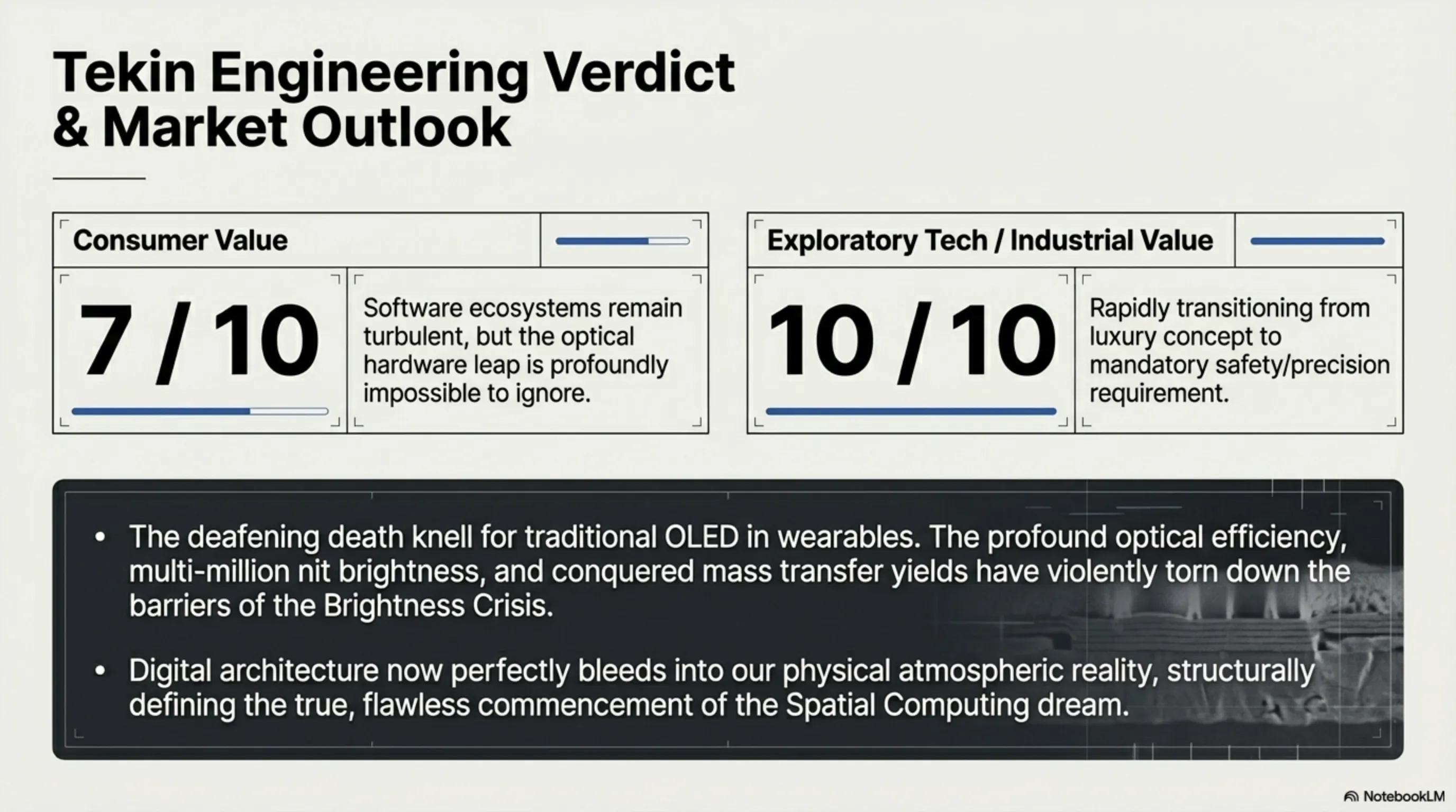
Final Editorial Verdict from the Tekin Engineering Desk: An Early, Brutal Farewell to OLED Panels
2026 Purchasing Value of AR Equipment for General Consumers: 7 out of 10 (First-generation mass-produced hardware inevitably grapples with highly turbulent software ecosystems and deeply fluctuating app support, yet the sheer undeniable hardware leap in optical capability makes it profoundly impossible to ignore.)
Exploratory Tech Value for Automotive and Elite Medical Industries: 10 out of 10 (The aggressive integration of MicroLED-powered HUD holographics and surgical MR overlays is rapidly transitioning from a high-end luxury concept to an absolutely critical, mandatory standardized safety and precision requirement across all elite smart machines.)
Final Tekin Architectural Analysis: The spectacular, undeniable triumph of MicroLED technology throughout 2026 was predicated upon one absolute, aggressively singular foundation: forcefully conquering the uncompromising physical limitations of quantum physics and eradicating the thermal vulnerabilities inherently plaguing organic OLED materials. Achieving multi-million nit brightness outputs alongside practically infinite contrast ratios within an optical panel whose physical dimensions aggressively refuse to exceed even half an inch, officially, violently tolls the deafening death knell for traditional OLED and archaic LCD formats within the rapidly expanding realm of portable wearable hardware. We are actively, currently witnessing the explosive dawn of a terrifyingly advanced technology that violently liberates the visual digital display from the deeply restrictive confines of a heavy glass rectangle gripped in your hand (the smartphone). This technology brutally and flawlessly projects critical digital telemetry and immersive volumetrics with stunning, breathtaking clarity directly and boundlessly upon the physical fabric of the environment surrounding the user; structurally defining the true, flawless commencement of the Spatial Computing dream.